Extreme Ultraviolet Lithography: The Hardest Machine Ever Commercialised
Modern semiconductor manufacturing relies on extreme ultraviolet lithography to etch features onto silicon at the scale of a few nanometres. This process requires a complex chain of high-energy plasma generation and precision reflective optics.
Key points
- ASML remains the sole provider of extreme ultraviolet scanners because the technology requires unprecedented precision in light source generation and mirror fabrication that others cannot replicate.
- The light source is created by hitting falling tin droplets with high-power lasers twice to produce a plasma emitting radiation at a wavelength of thirteen nanometres.
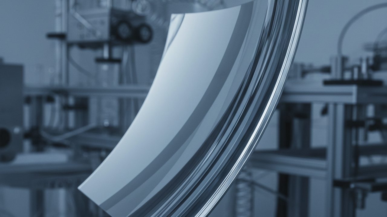
- Since standard glass absorbs extreme ultraviolet light, the system uses Bragg reflectors consisting of alternating molybdenum and silicon layers to steer the beam through a vacuum.
- Production capacity is constrained by a global supply chain of specialised components, including high-numerical-aperture lenses and custom laser systems, which take months to assemble and calibrate.
The physical scale of modern computation is determined by the properties of light. As silicon transistors are shrunk to increase performance and efficiency, the machines used to print them must work with increasingly shorter wavelengths. For decades, the semiconductor industry relied on deep ultraviolet light with a wavelength of 193 nanometres. This radiation is sufficient to define features down to a certain size, but as the industry moved towards nodes measured in single-digit nanometres, the diffraction of light became a fundamental barrier. When the features on a photomask are smaller than the wavelength of the light passing through them, the resulting image becomes blurred, much like trying to paint a miniature portrait with a household brush.
Extreme ultraviolet lithography, or EUV, is the technological response to this limit. It uses a wavelength of 13.5 nanometres, placing it closer to X-rays than to the visible spectrum. At this scale, the physics of light changes fundamentally. EUV radiation is absorbed by almost every material on Earth, including the air itself and the glass lenses traditionally used to focus light. Building a machine capable of harnessing this radiation required solving a series of engineering problems that many physicists initially considered insurmountable. The result is the most complex piece of manufacturing equipment ever sold, a system that costs roughly 150 million dollars and requires several Boeing 747s to transport.
The operation of an EUV scanner involves a series of transitions between states of matter and energy. It begins with a stream of molten tin and ends with a pattern etched onto a silicon wafer with atomic precision. The process is defined by the necessity of managing extreme heat and maintaining an almost perfect vacuum, as any stray molecule can obstruct the path of the photons. This technology is currently controlled by a single Dutch firm, ASML, which coordinates a global supply chain of specialised components, from German optics to American lasers.
The physical limits of optical lithography
To understand why EUV is necessary, one must consider the Rayleigh criterion, which defines the resolution limit of an optical system. The smallest feature a lithography machine can print is proportional to the wavelength of the light and inversely proportional to the numerical aperture of the lens. Throughout the 1990s and 2000s, engineers focused on increasing the numerical aperture and using resolution enhancement techniques, such as immersion lithography, where a layer of ultrapure water is placed between the lens and the wafer to bend light more sharply.
However, by the time the industry reached the 7-nanometre node, these methods had reached a point of diminishing returns. Continuing with 193-nanometre light required multiple patterning, a process where a single layer of a chip is printed in several passes. This increased the margin for error and slowed production significantly. The only remaining path forward was to reduce the wavelength of the light source itself. Moving from 193 nanometres to 13.5 nanometres represents a shift that allows for much finer resolution, but it also means that the light behaves less like a wave that can be easily refracted and more like a high-energy particle that is easily lost.
The transition to extreme ultraviolet light required an entirely new understanding of how matter interacts with high-energy photons.
Generating radiation from molten tin droplets
Generating 13.5-nanometre radiation at the scale required for mass production is a feat of high-speed plasma physics. There are no natural lasers or lamps that emit EUV light at the necessary intensity. Instead, the light is created by vaporising tin. Inside the source chamber of the lithography machine, a generator ejects 50,000 droplets of molten tin every second. These droplets, each roughly 30 micrometres in diameter, travel at speeds of roughly 70 metres per second.
As each droplet falls, it is struck by a high-power carbon dioxide laser. The process occurs in two stages. First, a low-energy pulse hits the droplet, flattening it into a pancake shape to increase its surface area. A second, much more powerful pulse then strikes the flattened tin, heating it to a temperature of several hundred thousand degrees Celsius. At this heat, the tin becomes a plasma. As the electrons in the plasma ions are stripped away and then fall back to lower energy states, they emit photons at a variety of wavelengths, including the desired 13.5-nanometre EUV light.
This plasma source is notoriously difficult to maintain. The debris from the vaporised tin can easily coat the internal optics, rendering them useless. To prevent this, the chamber is flooded with hydrogen gas, which reacts with the tin to form stannane, a gas that can be pumped away. Even with these measures, the source remains a volatile environment where the laser must hit its moving target with a precision of a few micrometres, 50,000 times a second, for hours on end.
The transition from refractive lenses to reflective mirrors
In traditional lithography, light is focused through a series of glass lenses. However, 13.5-nanometre light is absorbed by all known glass formulations. If an EUV beam were directed at a standard lens, the light would simply be absorbed and converted into heat. Consequently, EUV scanners must use a reflective system rather than a refractive one. Every component that the light touches, from the collector to the photomask to the final focusing elements, must be a mirror.
These are not standard mirrors. A typical silvered mirror reflects visible light well but is useless for EUV. Instead, the mirrors in an EUV system are Bragg reflectors, consisting of alternating layers of molybdenum and silicon. Each layer is only a few nanometres thick, precisely calculated so that the small amount of EUV light reflected at each interface interferes constructively. Even with this sophisticated design, these mirrors only reflect about 70 percent of the light that hits them. The remaining 30 percent is absorbed as heat, which can cause the mirrors to expand and distort.
The precision required for these mirrors is unprecedented. Manufactured primarily by the German company Zeiss, they are polished to a smoothness where the largest deviation from the intended shape is smaller than the diameter of a single atom. If the mirror were scaled to the size of a country, the highest hill would be less than a millimetre tall. This level of smoothness is necessary because any imperfection would cause the EUV light to scatter, ruining the pattern on the silicon wafer. Because the light must bounce off several of these mirrors before reaching the wafer, and 30 percent of the energy is lost at each bounce, the original light source must be incredibly bright to ensure enough photons reach the target.
Maintaining a vacuum for short-wavelength light
Because EUV light is absorbed by oxygen and nitrogen, the entire path of the light—from the tin plasma source to the silicon wafer—must be held in a high vacuum. This introduces significant engineering constraints. In previous generations of lithography, the air could be used to help cool the components and maintain a stable environment. In an EUV machine, the vacuum removes the possibility of convective cooling, meaning all heat must be managed through conduction or radiation.
The vacuum also complicates the handling of the silicon wafers and the photomasks. Any particle of dust that enters the system cannot be easily cleared, and in a vacuum, particles can behave in unpredictable ways, sometimes sticking to surfaces via electrostatic forces. To protect the photomask, which contains the master pattern for the chip, engineers developed a pellicle—a thin, transparent membrane that sits above the mask. This pellicle must be strong enough to survive the environment but thin enough not to absorb too much of the precious EUV light.
The vacuum system itself is vast, requiring a series of powerful pumps to maintain a pressure roughly one billion times lower than atmospheric pressure. Any leak or outgassing from the materials inside the machine would immediately cloud the optics and stop production. This requirement for a total vacuum, combined with the need for high-speed mechanical movement of the wafer stage, creates a machine that is as much a feat of vacuum engineering as it is of optics.
- The light source requires 40 kilowatts of laser power to produce just a few hundred watts of EUV light.
- Each mirror layer must be deposited with atomic-scale uniformity across a surface dozens of centimetres wide.
The coordination of these systems ensures that the final image projected onto the silicon is accurate to within a fraction of a nanometre. This precision allows for the creation of features so small that they are approaching the limits of the silicon crystal lattice itself. The transition to EUV has effectively extended the life of Moore’s Law, though it has done so at the cost of immense industrial concentration and complexity. The supply chain for these machines is so specialised that there are no alternative providers for many of the key subsystems, making the entire global semiconductor industry dependent on the continued success of this specific technological approach.
Atomic precision in molybdenum and silicon layering
The primary obstacle to using extreme ultraviolet light is that it does not reflect off conventional mirrors. At a wavelength of 13.5 nanometres, light is absorbed by almost all matter, including air and standard glass optics. To direct this light, engineers rely on Bragg reflectors, which are structures composed of alternating layers of two different materials. In EUV lithography, these layers are typically molybdenum and silicon.
Each mirror consists of approximately 40 to 50 pairs of these layers. The thickness of each layer is determined by the physics of constructive interference. For 13.5 nanometre light, a layer of silicon is roughly 4 nanometres thick, while a layer of molybdenum is roughly 3 nanometres thick. When light hits the boundary between these materials, a small fraction is reflected. By stacking dozens of these boundaries, the cumulative reflection reaches about 70 per cent. The remaining 30 per cent of the energy is absorbed as heat, which necessitates complex cooling systems to prevent the mirror from expanding and distorting the image.
Manufacturing these mirrors requires a process called ion beam sputtering. This involves bombarding a target material with ions to knock atoms loose, which then settle onto the mirror substrate. The uniformity required is extreme. A deviation in thickness of a few picometres, the width of a fraction of an atom, can shift the phase of the reflected light and ruin the focus. The surface of the mirror must be so smooth that if it were scaled to the size of a country, the highest hill would be less than a millimetre tall.
Computational correction for optical distortions
Even with near-perfect mirrors, the physics of EUV light introduces distortions that must be corrected before the light ever touches the silicon. Because the wavelength is so short, the interaction between the light, the mask, and the photoresist is prone to stochastic effects. These are random variations in where individual photons land, which can lead to rough edges on the circuits or missing connections.
To compensate for these effects, engineers use computational lithography. This involves simulating the entire optical path in reverse. The design of the chip is not what is actually printed on the photomask. Instead, the mask features are distorted into strange, curved shapes that look nothing like a circuit. These shapes are calculated so that, after the light has bounced off multiple mirrors and passed through the lens assembly, the resulting interference pattern on the wafer matches the intended circuit design.
This process requires massive amounts of computing power. Every time a chip design is finalised, a supercomputing cluster runs algorithms to determine the optimal mask pattern. The software must account for the specific characteristics of the EUV light source, the flare caused by the mirrors, and the chemical reaction of the photoresist. This is no longer just an optical problem; it is a mathematical one, where the physical hardware and the digital simulation are inseparable.
The mask is essentially a mathematical inverse of the optical system, designed to counteract the unavoidable blurring of extreme ultraviolet light.
The industrial bottleneck of single-source components
The production of EUV machines is perhaps the most concentrated industrial process in history. A single Dutch firm, ASML, holds a monopoly on the assembly of these systems. However, the concentration extends deep into the sub-components. The laser system required to hit the tin droplets is produced by a single German company, and the mirrors are manufactured exclusively by another. There are no secondary suppliers capable of meeting the specifications.
This creates a fragile global infrastructure. Each machine costs roughly 150 million dollars and contains over 100,000 parts. The logistics of building and shipping these units involve chartered cargo planes and years of advance planning. Because the cost of entry is so high, no other company has been able to develop a competing EUV system. The research and development took three decades and billions of dollars in investment, much of it funded by the semiconductor manufacturers who now buy the machines.
This single-source model means that any disruption in the supply chain or any failure in the technical roadmap has immediate consequences for the entire electronics industry. If a new generation of optics cannot be produced at scale, the steady increase in computing power that has defined the last fifty years could stall. The industry has effectively bet its entire future on the continued engineering success of a few thousand specialists in Europe and North America.
Current engineering challenges for high numerical aperture
The next step in EUV technology is High Numerical Aperture, or High-NA. To print even smaller features, the industry needs to increase the angle at which light hits the wafer. This requires larger mirrors and a complete redesign of the internal housing of the machine. The goal is to move from the current resolution of 13 nanometres down to less than 8 nanometres.
High-NA machines present a new set of physical problems. Because the light hits the mask at a steeper angle, the shadows cast by the mask features become a significant issue. To fix this, engineers are moving to anamorphic optics, where the image is magnified by different amounts in the horizontal and vertical directions. This allows the machine to maintain resolution without requiring masks that are impossibly large.
The weight and size of these new machines are significant. A High-NA EUV system is roughly the size of a double-decker bus and weighs over 200 tonnes. The structural engineering required to keep such a massive machine stable while its internal parts move with nanometre precision is unprecedented. Even the vibrations from a nearby road or the hum of a ventilation system must be actively cancelled out by magnetic levitation and sophisticated dampening systems.
Limits of silicon scaling and the next decade
The push toward smaller features is reaching a point where silicon atoms themselves are the constraint. A silicon atom is roughly 0.2 nanometres wide. The gate oxides in the most advanced transistors are now only a few atoms thick. At this scale, quantum tunnelling becomes a major problem, as electrons can simply leak through barriers that are supposed to stop them.
EUV lithography has provided a path to continue scaling for the next ten years, but the path beyond that is unclear. There is active research into using shorter wavelengths, such as Soft X-rays, but this would require entirely new materials and light sources. Another possibility is moving away from silicon to two-dimensional materials like molybdenum disulfide, which can be made into thinner, more efficient channels.
If the industry cannot find a way to circumvent the physical limits of the silicon lattice, the era of exponential growth in transistor density will come to a structural end.
The current consensus is that High-NA EUV will be sufficient to take the industry to the 2-nanometre node and perhaps the 1.4-nanometre node by the end of the decade. Beyond that, the engineering community is divided. Some argue that vertical stacking of transistors, known as 3D integration, will be more important than further shrinking the features themselves. Others believe that new forms of lithography, perhaps involving multiple electron beams rather than light, could eventually replace EUV.
What is established is that EUV is the most complex tool ever put into mass production. It works by mastering forces that were once considered laboratory curiosities. What remains contested is whether the enormous financial cost of these machines can be sustained by any but the largest three or four chipmakers. If the cost of the next generation of machines doubles again, the economic incentive to shrink chips may vanish before the physical limit is ever reached. The future of computing depends not just on whether we can build these machines, but on whether the global economy can continue to afford the precision they demand.